Intel is making a very public—and very expensive—point lately: the future of chips is not just about smaller transistors. It’s about how you stitch multiple pieces of silicon together so they behave like one monster processor without turning your data center into a space heater with networking cables.
That’s the core theme behind the original Ars Technica story (RSS source) titled “Intel is going all-in on advanced chip packaging,” by Ryan Smith. This article takes that foundation and expands it into the bigger industry picture: why packaging has become the new battleground for AI and HPC, what Intel’s EMIB and Foveros families actually do, what the bottlenecks are (spoiler: it’s not only EUV scanners), and where this “systems foundry” narrative fits into Intel’s comeback—or reinvention—attempt.
If you’re a normal human being who just wants a laptop that doesn’t sound like a leaf blower: don’t worry. Packaging still matters to you, too. It’s one of the reasons today’s CPUs and GPUs are increasingly “chiplets” rather than one big slab of silicon—and it’s how AI accelerators keep cramming in more high-bandwidth memory (HBM) without collapsing under the weight of physics, yields, and economics.
Packaging: The Part of the Chip Story We Used to Skip
For decades, semiconductor storytelling was basically a single plotline: “transistors get smaller.” Moore’s Law was the headline; the fab was the hero; lithography was the cinematic special effect. Packaging was the end credits—important, sure, but you only read it when you were waiting to see if there’s a post-credit scene.
That’s not true anymore. As Intel Foundry boss Naga Chandrasekaran told WIRED, even the term “advanced packaging” is relatively new in mainstream chip discourse, and the industry’s needs changed as chips became denser, more complex, and more memory-hungry. citeturn2view2
In the AI era, packaging is no longer “how do we protect the die and connect pins.” It’s system architecture. It’s the difference between a GPU that scales and one that is limited by memory bandwidth, interconnect energy, or substrate warpage. It’s also, increasingly, the difference between shipping a product this year versus being stuck in a queue behind the next hyperscaler’s order for CoWoS capacity.
The uncomfortable truth: leading-edge AI chips are assembled, not just fabricated
Modern high-end processors are increasingly disaggregated: you build multiple tiles (CPU cores, GPU compute, cache, I/O, sometimes even analog bits), then you connect them with short, fat, low-power links inside one package. This approach improves yield (smaller dies mean fewer defects per die), allows mixing of process nodes, and makes it easier to scale designs across product families.
Intel explicitly frames its foundry business as a bundle of capabilities that includes wafer fabrication and advanced packaging. In its 2025 annual filing, Intel describes foundry offerings as including wafer fab, advanced packaging, chiplet integration, and design enablement services—highlighting packaging as strategic, not auxiliary. citeturn3view0
Intel’s Pitch: “Enter and Exit the Highway”
One of the more interesting bits from recent reporting is Intel’s positioning of packaging as a modular service. At its Rio Rancho, New Mexico site (Fab 9), Intel’s leadership described how a customer can effectively use Intel as one stage in a broader supply chain: bring wafers from elsewhere, do advanced assembly at Intel, or mix Intel with an OSAT partner. WIRED quoted Intel describing this as the ability to “enter and exit the highway” during manufacturing. citeturn2view2
This matters because the packaging market has a trust problem and a capacity problem at the same time:
- Capacity problem: AI demand has stressed advanced packaging throughput industry-wide. If your HBM-centric accelerator needs a particular integration flow, the back-end can become the schedule limiter—even when wafer supply is available.
- Trust problem: Intel is a foundry supplier and a competitor in several segments. Some customers may hesitate to announce partnerships until Intel demonstrates consistent delivery and scale, and there are concerns about broader market dynamics with other suppliers. citeturn2view2
Still, Intel’s “pick the pieces you want” model is pragmatic. In 2026, no one serious thinks the semiconductor supply chain is going back to a clean single-vendor story. The question is whether Intel can be the go-to second option—and eventually, for some customers, the first.
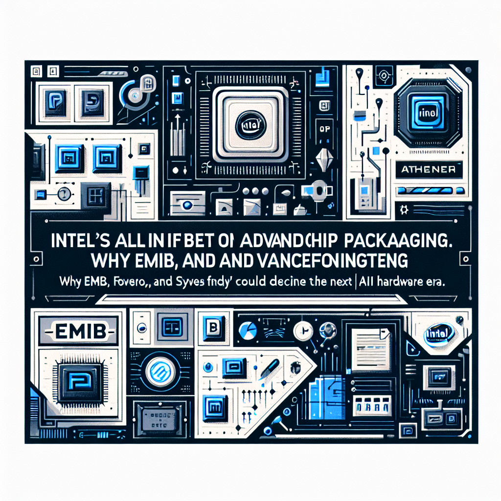
EMIB and Foveros: The Two Names Intel Wants You to Remember
Intel’s modern packaging branding mostly lives in two families:
- EMIB (Embedded Multi-die Interconnect Bridge) for 2.5D-style bridging between dies—often for logic-to-logic or logic-to-HBM connections.
- Foveros for stacking and more complex heterogeneous integration—2.5D variants and 3D die stacking.
Intel emphasizes that EMIB has been in high-volume production since 2017, and that EMIB-T adds through-silicon vias (TSVs) to the bridge for bandwidth scaling and improved power delivery characteristics. citeturn2view0turn3view0
What EMIB actually is (and why it’s not “just an interposer”)
Classic 2.5D integration often uses a silicon interposer: a big slab of silicon that sits under multiple dies, routing signals between them. It works well, but it can be expensive and has size limitations tied to reticle and manufacturing considerations.
EMIB takes a different route: rather than placing everything on a full interposer, Intel embeds smaller silicon bridges directly into the package substrate to connect dies “shoreline-to-shoreline.” Intel positions EMIB as a cost-effective, high-density way to connect complex dies, including logic and HBM. citeturn2view0
The newer EMIB-T variant adds TSVs to the bridge, and Intel says this can ease IP integration from other packaging designs—translation: “We can help you port designs that were built with someone else’s packaging assumptions.” citeturn2view0
Foveros: stacking done in multiple flavors
Foveros started as Intel’s banner for 3D stacking, but it has become a family with multiple approaches for different cost/performance targets. Intel’s current Intel Foundry packaging page outlines several notable branches:
- Foveros-S (2.5D): optimized for cost/performance; uses a silicon interposer and is described as production proven since 2019.
- Foveros-R (2.5D): uses an RDL (redistribution layer) interposer; Intel calls it production ready in 2027.
- Foveros Direct (3D): copper-to-copper hybrid bonding interface for ultra-high bandwidth and low power; can be combined with EMIB 3.5D solutions.
Those details come straight from Intel Foundry’s public packaging overview, which also underlines that the company is trying to cover a spectrum—from cost-sensitive client designs to bleeding-edge data center integration. citeturn2view0
Why Now? Because AI Is a Packaging Problem (Too)
AI chips have become memory systems with compute attached. Training and inference at scale are constrained by moving data, not just doing math. So you see designs with large numbers of HBM stacks sitting close to compute tiles, linked by short, dense interconnects that need to be fast, power-efficient, and manufacturable in volume.
This is where packaging becomes existential. When you see the industry obsessing over CoWoS, SoIC, hybrid bonding, and 3D stacking, it’s not because chip engineers got bored. It’s because the math says that if you can reduce interconnect energy per bit and increase bandwidth density, you unlock whole new performance-per-watt regimes.
Packaging capacity is a competitive moat
In a recent wave of coverage, analysts and media have pointed to the strain on leading-edge packaging capacity in the ecosystem, with AI demand stretching supply. That creates an opening for anyone who can deliver high-yield advanced assembly at scale, particularly in geopolitically desirable locations.
Intel’s attempt to stand out here is two-fold:
- Technology differentiation (EMIB variants, Foveros variants, and the ability to mix 2.5D/3D in one package).
- Manufacturing footprint (geo-diverse assembly/test plus U.S. capacity).
Intel’s own filings explicitly call out New Mexico as its key advanced packaging facility and note that the company is building a new advanced packaging facility in Malaysia, while emphasizing the importance of reliable capacity across sites to meet demand. citeturn3view0
The New Mexico Packaging Hub: Fab 9 as a Strategic Asset
Intel opened Fab 9 in Rio Rancho, New Mexico as a high-volume advanced packaging site, describing it as the first operational site for mass production of Intel’s 3D advanced packaging technology and its first co-located high-volume advanced packaging site (end-to-end manufacturing efficiency). citeturn2view1
It also matters politically and economically. Intel’s Newsroom announcement highlighted a $3.5 billion investment in Rio Rancho, with job creation figures cited for both direct Intel employment and construction work. citeturn2view1
In practical terms, New Mexico is part of Intel’s argument that it can offer something that many customers want: a packaging option in the United States, integrated into a broader manufacturing network.
The reality check: packaging scale is not a switch you flip
As analyst Jim McGregor (Tirias Research) told WIRED, packaging isn’t as simple as declaring a wafer-start number. The complexity is in the flow, tooling, yield, and deal-making. citeturn2view2
That’s an important reminder because “advanced packaging” is a multi-step choreography involving die sort, known-good-die strategies, bonding, substrate handling, thermal management, and final test. When it works, it’s magic. When it doesn’t, it’s a very expensive pile of scrap and schedule slips.
Malaysia Expansion and the “Geo-Diverse” Play
Intel has long-standing operations in Malaysia, and recent reporting indicates it’s expanding advanced packaging/assembly/test capacity there as well. WIRED reported that Malaysia’s prime minister, Anwar Ibrahim, referenced an Intel expansion that includes advanced packaging, and an Intel spokesperson confirmed additional assembly and test capacity in Penang amid demand for Intel Foundry packaging solutions. citeturn2view2
From a strategy standpoint, Intel wants to be able to tell customers: “We can build and assemble your chips across a resilient network.” In its annual filing, Intel lists key assembly/test facilities in China, New Mexico, Vietnam, and Malaysia, and notes a new advanced packaging facility being built in Malaysia. citeturn3view0
This isn’t just about logistics. It’s about risk management: geopolitics, export controls, supply shocks, and the sheer fragility of concentrated capacity in one region for key back-end steps.
Advanced Chiplet Test: The Unsexy Problem That Can Kill Yields
When you move from one monolithic die to multiple chiplets, you don’t get to pretend yield is a solved problem. You’ve traded one big yield risk for many smaller ones—and then added an assembly yield layer on top.
Intel Foundry’s packaging page spends real estate on Advanced Chiplet Test, emphasizing known-good-die strategies and multiple phases: wafer sort, die sort, final test, and system-level test. The idea is straightforward: the more chiplets you pack together, the more you need confidence that each one is good before you bond it into an expensive multi-die assembly. citeturn2view0
This is one of those areas where Intel’s decades of high-volume CPU manufacturing culture could help—if it translates cleanly into foundry customer workflows and toolchain expectations.
EMIB 3.5D: When 2.5D Meets 3D in One Package
Intel also talks about EMIB 3.5D, which combines EMIB and Foveros in the same package—effectively enabling multiple 3D stacks connected through 2.5D bridges. Intel positions this as useful for heterogeneous systems combining many dies and 3D stacks together. citeturn2view0
This type of hybrid approach is key to where AI hardware is headed: a mix of compute tiles, SRAM/cache tiles, I/O tiles, and a whole lot of HBM. Not everything needs to be stacked; not everything can be placed side-by-side efficiently. So the next generation of packages looks less like “a chip” and more like “a neighborhood plan.”
The Competitive Context: TSMC’s CoWoS, SoIC, and Why Intel Wants a Seat at That Table
No discussion of advanced packaging is complete without mentioning TSMC, which has built a massive business around integrating dies with technologies like CoWoS and SoIC. WIRED’s overview captures how TSMC pitched customers on handling both front-end wafer manufacturing and back-end packaging—an end-to-end convenience that became especially attractive as AI chips scaled up. citeturn2view2
Intel’s counter-pitch is differentiation (EMIB’s bridge approach being “surgical,” as a former Intel employee described it to WIRED) and flexibility in supply chain integration. citeturn2view2
But let’s be honest: there’s also a meta-competition here. Packaging is a place where Intel can credibly claim unique strengths, even while it works to regain leadership in wafer process technology. It’s a battleground where “good enough, available, and scalable” can win business, even if you’re not the default choice for everyone.
What This Means for Real Products: Chiplets Everywhere
It’s easy to get lost in the acronyms and forget the practical endpoint: shipping silicon that people can buy.
Intel’s own corporate filing notes that disaggregated architectures and leading-edge packaging are now common across many advanced products (including those of prospective foundry customers), and explicitly ties EMIB and Foveros investments to this trend. citeturn3view0
In other words: even if you never buy an Intel GPU, you may still end up using a device that relies on Intel packaging technology—if Intel succeeds in selling advanced packaging services to third parties.
Why chiplets keep winning
- Yield and cost: Smaller dies typically yield better, lowering cost for a given capability level.
- Mixing nodes: Put compute on an advanced node, keep I/O on an older cheaper node.
- Reuse and scaling: Reuse chiplets across SKUs; scale by adding more chiplets rather than designing a new monolith.
Packaging is what makes these benefits possible without introducing unacceptable latency, power overhead, or reliability issues.
The Foundry Angle: Packaging as a Wedge Into Customer Relationships
Intel’s bigger business goal is to grow a customer-centric foundry model. In its filing, Intel describes the foundry strategy as long-term and built on trust, emphasizing quality, reliability, and yield as essential. citeturn3view0
Packaging can function as a wedge because it doesn’t always require a customer to jump fully into Intel’s wafer process from day one. If a company is locked into another wafer supplier but needs additional packaging capacity or wants a U.S.-based back-end path, Intel can attempt to win that slice of the workflow. Over time, that can expand into deeper engagements—assuming Intel executes well.
From the customer perspective, the ideal scenario looks like this:
- Use the best wafer process for each chiplet (which could be Intel, TSMC, Samsung, or a mature-node foundry).
- Use the best packaging tech and capacity available.
- Avoid being bottlenecked by one vendor’s queue or geopolitics.
Intel is trying to be a credible answer to “who else can package my HBM-heavy design at scale?”
The Hard Parts: Thermals, Warpage, and Reliability (a.k.a. Physics Is Still Employed)
Advanced packaging isn’t just fancy wiring. It’s also a set of mechanical and thermal problems that get worse as packages get larger, power density climbs, and materials expand/contract differently.
Every extra die and every extra HBM stack is another source of heat, another contributor to stress, and another opportunity for something to go wrong during bonding or operation. That’s why packaging roadmaps increasingly include not just interconnect density targets, but also substrate innovations, thermal approaches, and test methodologies.
Academics and industry continue to publish work on the structural and thermal trade-offs in 2.5D integration, reflecting how placement and thermal modeling can become first-order design constraints in chiplet systems. citeturn1academia16
So… Is Intel Really “All In”? Reading Between the (Cleanroom) Lines
The phrase “all in” gets thrown around a lot in tech, usually by people who are absolutely not all in (they still have a backup plan, a slide deck, and a consultancy retainer).
But Intel’s actions and disclosures make it clear packaging is one of the company’s chosen leverage points:
- It is investing in high-volume advanced packaging sites like Fab 9 in New Mexico. citeturn2view1
- It is expanding and diversifying assembly/test capacity, including Malaysia. citeturn2view2turn3view0
- It is publicly marketing packaging as a first-class foundry offering with a broad portfolio (2D, 2.5D, 3D; multiple Foveros variants; EMIB and EMIB-T; test services). citeturn2view0
- It is framing advanced packaging as key to disaggregated architectures for both internal products and external foundry customers. citeturn3view0
That’s not a side quest. That’s a core quest with optional boss fights against physics, supply chain constraints, and customer skepticism.
Implications: Who Benefits If Intel Pulls This Off?
If Intel succeeds in scaling advanced packaging as a competitive foundry service, the ripple effects could be meaningful:
- AI hardware startups and “second-tier” accelerator teams could gain alternatives when premier packaging lines are booked solid.
- Hyperscalers could diversify packaging risk and potentially bring some advanced integration closer to U.S. soil for supply-chain resilience.
- The broader ecosystem could see faster adoption of standards like UCIe (Intel explicitly references driving industry standards in its packaging overview), enabling more mix-and-match chiplet strategies over time. citeturn2view0
On the flip side, if Intel stumbles—on yields, ramp, or customer confidence—the company risks having built impressive facilities that don’t translate into a steady stream of third-party revenue. And in semiconductors, underutilized capacity is the kind of “oops” that shows up on earnings calls with the subtlety of a dropped server rack.
What to Watch in 2026–2028
Here’s what I’ll be watching over the next couple of years if you want the “tell me whether this is working” checklist:
- Named external customers for advanced packaging services—especially customers willing to say so publicly.
- EMIB-T scaling in 2026, which Intel expects to ramp starting in 2026 per its annual filing. citeturn3view0
- Foveros variant timelines: Intel targets Foveros-B and Foveros-R for high-volume manufacturing in 2027, and notes hybrid-bonding support planned with Intel 18A-PT in 2028 for Foveros Direct in its filing. citeturn3view0
- Operational proof that Intel’s “enter and exit the highway” model works smoothly across supply-chain boundaries (wafer from vendor A, packaging at Intel, final test elsewhere).
- Geopolitical and policy tailwinds that might encourage domestic packaging capacity—especially for government and enterprise customers seeking U.S.-based options.
Bottom Line
Intel’s big packaging push isn’t a quirky detour from the real story of process nodes. It’s a recognition that the modern “chip” is increasingly a system inside a package. For AI accelerators, packaging is where bandwidth density, power efficiency, and manufacturability collide—often violently.
Ars Technica’s reporting (again: original source by Ryan Smith) captured the company’s all-in messaging. The broader industry context suggests the bet is rational: demand for advanced packaging is growing, the ecosystem is strained, and heterogeneous integration is how the next decade of compute scales.
The remaining question is execution. Intel can’t simply invent acronyms faster than its competitors (though it is, admittedly, trying). It has to deliver yields, volume, and customer confidence—because the future of high-end silicon will be decided as much by what happens after the wafers are made as it is by what happens during lithography.
Sources
- Ars Technica (Ryan Smith): “Intel is going all-in on advanced chip packaging”
- Intel Foundry: Advanced Packaging Innovations (EMIB, EMIB-T, Foveros variants, Advanced Chiplet Test)
- Intel Newsroom: “Intel Opens Fab 9 in New Mexico”
- WIRED: “The Ridiculously Nerdy Intel Bet That Could Rake in Billions”
- Intel (INTC) SEC filing (Form 10-K HTML): Foundry strategy, EMIB/EMIB-T and Foveros roadmap notes
- arXiv paper: “STAMP-2.5D: Structural and Thermal Aware Methodology for Placement in 2.5D Integration”
Bas Dorland, Technology Journalist & Founder of dorland.org